Using EasyEDA for IoT PCB Design: Step-by-Step Online Tutorial
Introduction: Why This Tutorial?
Designing PCBs for IoT doesn’t have to be intimidating. Whether you’re a student building your first smart project, or an enthusiast prototyping connected devices, EasyEDA online makes it possible to bring your circuit ideas to life without any software installation.
This guide will help you:
- Understand the EasyEDA pcb design environment
- Simulate circuits with easyEDA circuit simulator
- Design and export PCBs using the easyeda online pcb design workflow
- Learn how to avoid beginner mistakes with real-world IoT examples
Let’s begin from scratch and walk you through this journey.
What is EasyEDA Online?
EasyEDA stands for Easy Electronic Design Automation. It is a free online EDA tool that combines powerful features of a schematic editor, circuit simulator, and PCB layout in a single web platform.
Key Benefits:
- 100% browser-based – no installation required
- Real-time project saving to the cloud
- Compatible with IoT modules like ESP32, ESP8266, and sensors
- Direct integration with JLCPCB for quick manufacturing
- Visual circuit simulation using easyEDA circuit simulator
This makes easyEDA online simulator ideal for both educational and professional use.
Core Features of EasyEDA for IoT Developers
| Feature | Description |
|---|---|
| Schematic Capture | Drag & drop components from an extensive library |
| PCB Design Editor | Convert schematic to PCB layout with auto-routing |
| Online Circuit Simulation | Test your IoT circuits before manufacturing |
| Component Search | Built-in LCSC library with thousands of parts |
| Cloud Collaboration | Share your project via links for team work |
Step-by-Step EasyEDA Online PCB Design Guide
Follow these steps to go from concept to a working IoT PCB design using EasyEDA online.

1. Sign Up & Create a Project
- Go to https://easyeda.com
- Sign up with email or log in using Google
- Click on “New Project” > Enter your project name > Select Schematic Design
Now you’re ready to create your circuit!
2. Navigating the Dashboard
When your project opens, you’ll see:
- Toolbar (left): Wires, components, text, nets
- Workspace (center): Drawing area for circuits
- Component Library (right): Search parts from built-in EasyEDA or LCSC
Tip: Use search terms like “ESP8266”, “Relay Module”, “DHT11”, “LED”, or “Power Jack” to quickly add parts for IoT designs.
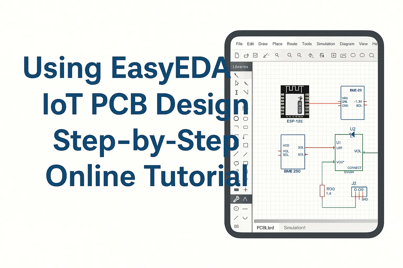
3. Create Your Circuit Schematic
Let’s build a Wi-Fi-based smart relay switch using ESP8266.
Components Needed:
- ESP8266 WiFi module
- Relay module
- BC547 Transistor
- 1N4007 Diode
- Resistor (10k)
- Power Supply (5V)
Steps:
- Drag components into the workspace.
- Connect using ‘Wire’ tool or shortcut key ‘W’.
- Assign labels like
GPIO0,VCC,GND,IN1. - Add test points or headers for programming/debugging.
Keep power and ground connections tidy for better layout later.
4. Simulate Circuit in EasyEDA Circuit Simulator
Once your schematic is ready, simulate it using the easyEDA circuit simulator.
Steps:
- Click “Simulate” from the top menu.
- Add voltage sources (e.g., 5V DC supply).
- Set probes to GPIO, collector pin, relay input.
- Define simulation type (DC, AC, Transient).
- Run simulation.
You’ll see how voltages flow through your design — without needing physical components!
5. Convert Schematic to PCB Layout
When the circuit works as expected, click “Convert to PCB”.
- Set board dimensions (e.g., 70x50mm)
- Position components manually
- Use the ‘Route’ tool to draw copper connections
- Add text like project name, version, and your initials
Add mounting holes if your PCB will go into an enclosure.
6. Use Auto-Routing (or Manual for Better Results)
Click Tools > Auto Router to let EasyEDA do the hard work.
You can also route signals manually to optimize:
- Shorter tracks for critical signals
- Separate analog and digital grounds
- Wide traces for power and GND
Design Tips:
- Avoid 90° trace angles (use 45°)
- Place decoupling capacitors near ICs
- Keep relay away from MCU to avoid interference
7. Run Design Rule Check (DRC)
Before finalizing your PCB, go to Tools > Design Manager > DRC Errors.
Look out for:
- Unconnected nets
- Clearance issues
- Missing copper connections
Ignoring these can result in failed boards during manufacturing.
8. Export Gerber Files & Order PCB
Click Fabrication Output > Gerber Export.
You can either:
- Download Gerber ZIP and upload to any manufacturer
- Click “Order at JLCPCB” and choose solder mask color, thickness, and quantity
Boards can arrive in 5–7 days for most locations!
Real IoT Project Examples Made with EasyEDA
Here are beginner-friendly IoT ideas to start designing with EasyEDA:
| Project Idea | Modules Used | Description |
| Smart Door Lock | ESP8266 + RFID | Lock/unlock using cloud + RFID |
| Gas Leak Detector | MQ-2 + ESP8266 + Buzzer | Alert on gas detection |
| Smart Irrigation | Soil Sensor + ESP8266 | Automated plant watering |
| Weather Station | DHT11 + LCD + WiFi | Display weather stats with IoT |
| Home Automation | Relay + ESP8266 | Control lights/fans via Wi-Fi |
EasyEDA vs Other PCB Tools
| Feature | EasyEDA Online | KiCad | Fritzing |
|---|---|---|---|
| Installation | No | Yes | Yes |
| Cloud Access | Yes | No | No |
| Circuit Simulation | Yes | Basic | No |
| IoT Components Support | Yes | Yes | Moderate |
| Built-in Ordering | Yes | No | No |
| Ease for Beginners | High | Medium | High |
If you’re new to electronics, EasyEDA online pcb design offers the smoothest learning curve.
Best Practices for IoT PCB Design
- Always include bypass capacitors on power lines
- Separate digital and analog sections
- Use ground plane to reduce noise
- Label GPIOs clearly for firmware reference
- Allow programming headers or USB for firmware flashing
These practices ensure your IoT PCB is robust, functional, and scalable.
Conclusion
EasyEDA online provides a powerful platform that combines circuit design, simulation, and PCB manufacturing — all in your browser. Whether you’re building a home automation system or a sensor-based application, mastering EasyEDA pcb design will significantly accelerate your IoT development journey.
You now know how to:
- Create schematics
- Simulate circuits using easyEDA online simulator
- Design and export PCBs using easyEDA online pcb design
So, what’s your next smart idea?
See also: How to Design IoT Dashboard using Node-RED: Step-by-Step Tutorial
Frequently Asked Questions (FAQs)
Q1. What is EasyEDA used for?
EasyEDA is used for schematic creation, PCB layout, and circuit simulation – all online.
Q2. Can I simulate IoT circuits in EasyEDA?
Yes, the easyEDA circuit simulator allows simulation of analog and digital circuits.
Q3. Is EasyEDA good for beginners?
Absolutely! It has an intuitive interface and thousands of components for IoT.
Q4. Is it really free?
Yes, EasyEDA offers free access with optional paid plans for advanced collaboration.
Q5. How do I manufacture my EasyEDA PCB?
You can export Gerber files or order directly from JLCPCB with one click.
See also: Top 5 Best IoT Simulation Tools Online (No Hardware Needed)
Ready to Explore More? Let’s Build Smarter Together!
🔔 Subscribe to Our YouTube Channel » for IoT video Tutorials.
🌐 Start Learning IoT Basics Now » and What is IoT? – Introduction to IoT and IoT Architecture: 4 Essential IoT Layers Simplified for Beginners on IoTDunia.com! and Check out Top IoT Applications in Real World – Smart Use Cases 2025, IoT career guide 2025, Best Projects on IoT for Beginners
👉 Have questions? Drop them in the comments!
💡 Start small, stay curious, and make your world smarter—one device at a time.